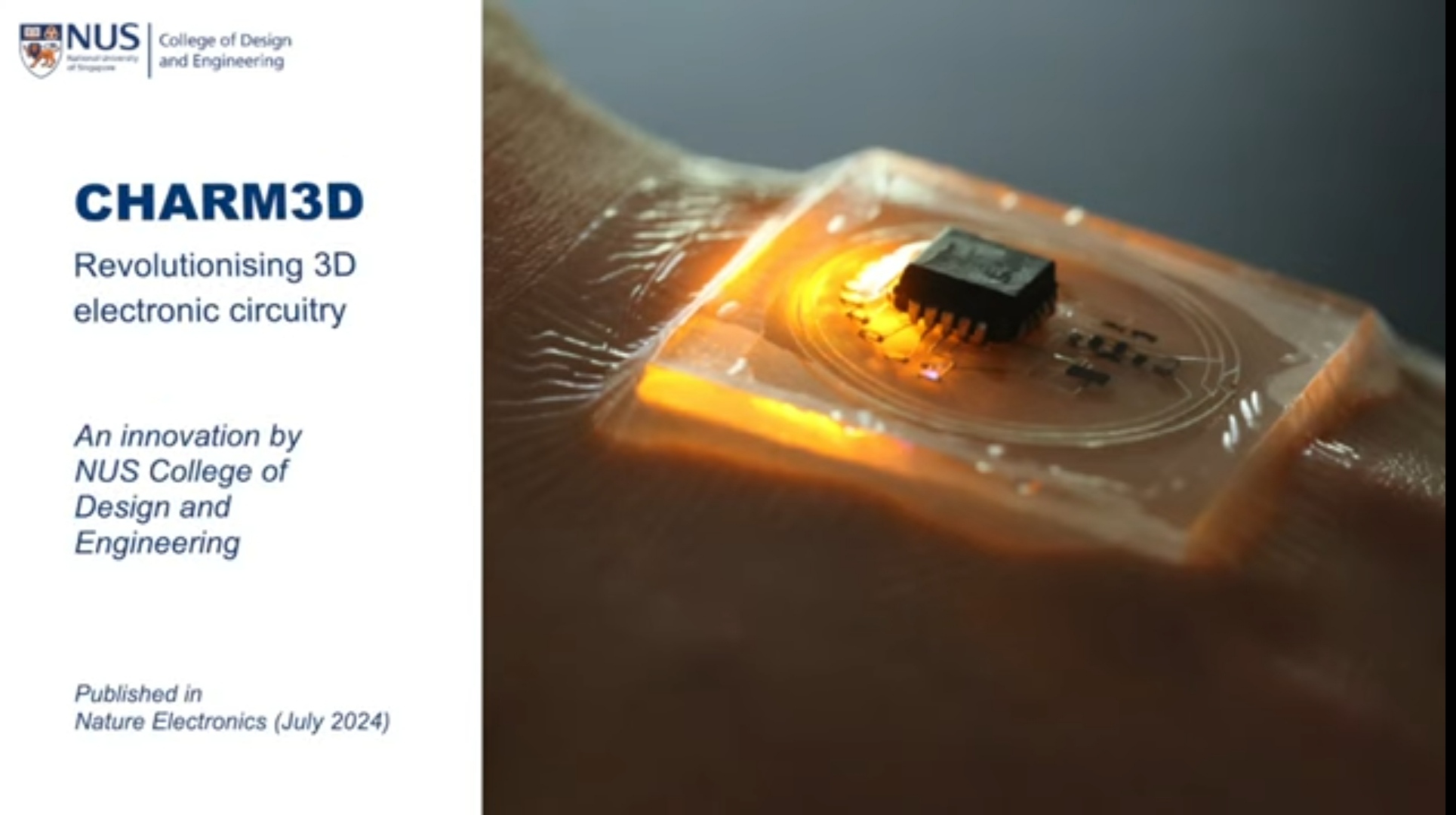
NUS researchers have developed a new technique for creating 3D circuits for advanced electronics
A Singapore team has developed a novel 3D printing technique for three-dimensional circuits.
CHARM3D facilitates the efficient printing of free-standing 3D structures with excellent electrical conductivity, self-healing properties, and recyclability, which is highly beneficial for electronics used in healthcare, communications, and security.

Traditional printed circuit boards are typically confined to being flat and two-dimensional. However, researchers from the National University of Singapore have advanced circuit printing into the third dimension with an innovative technique known as CHARM3D. Not only are these printed circuits three-dimensional, but they also possess the ability to self-heal.
By adopting a vertical approach rather than remaining flat, components can be stacked, resulting in significantly smaller electronic devices – a desirable feature in today’s market where compact and sleek designs are preferred. Existing methods like direct ink writing (DIW) face challenges in achieving 3D circuitry due to the need for support materials and the slow, viscous nature of composite inks used.

CHARM3D employs a different strategy by leveraging the unique properties of Field’s metal, an alloy of indium, bismuth, and tin. With a low melting point of about 62°C, this alloy flows smoothly and solidifies quickly. These characteristics allow CHARM3D to print extremely smooth and uniform 3D metal microstructures that are 100-300 microns wide – comparable to the width of a few human hairs. The printed structures can include cubic frameworks, vertical letters, and scalable helixes.
Additionally, these printed structures have self-healing capabilities. If the circuit is scratched or deformed, heating it past the alloy’s low melting point will allow it to re-solidify into its original form, enhancing durability and recyclability.
The potential applications of CHARM3D are vast. The high resolution, rapid printing speed (up to 100 millimeters per second), and ability to create complex 3D shapes make it suitable for a wide range of innovative uses.
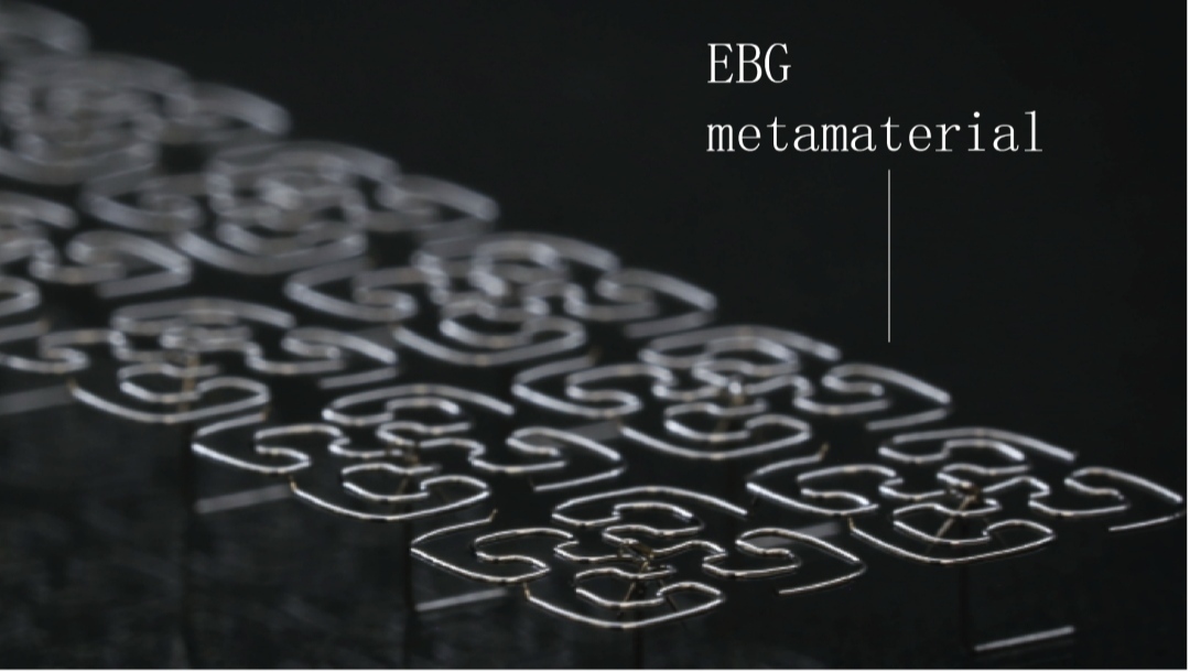
A major application identified by the researchers is in healthcare. For instance, smart clothing with 3D-printed sensors could monitor vitals without direct skin contact. It could also improve medical imaging, such as using microwaves for early breast cancer detection. The team has already demonstrated the technology by creating a wearable, battery-free temperature sensor, antennas for wireless vital sign monitoring, and metamaterials for manipulating electromagnetic waves.
Benjamin Tee, an associate professor leading the research, stated, “By offering a faster and simpler approach to 3D metal printing for advanced electronic circuit manufacturing, CHARM3D holds significant promise for the large-scale production and widespread adoption of complex 3D electronic circuits.”
While there is still more work to be done, including applying CHARM3D to other metals and structural applications, the team is exploring commercialization to broaden industrial adoption. The complete research findings are available in a paper published in Nature.
Next Step-
The research team envisions that this technique can be extended to other types of metals and structural applications. The team is also looking for opportunities to commercialise this unique approach for metal printing.


